연구
Research Outcome
미래를 창조하는 포스텍 화학공학과
Vapour-deposited high-performance tin perovskite transistors
- Title of paper
- Vapour-deposited high-performance tin perovskite transistors
- Author
- [노용영교수님 연구실] 열증착 고성능 주석 페로브스카이트 트랜지스터
- Publication in journal
- Nat. Electron. 8, 403-410 (2025).
- Publication date
- 20250428
[Abstract]
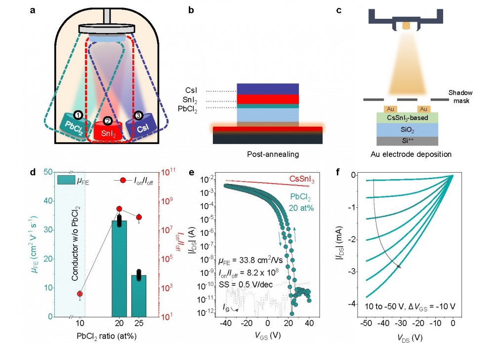
Solution-processed tin (Sn2+)-halide perovskites can be used to create p-channel thin-film transistors (TFTs) with performance levels comparable with commercial low-temperature polysilicon technology. However, high-quality perovskite film deposition using industry-compatible production techniques remains challenging. Here we report the fabrication of p-channel Sn2+-halide perovskite TFTs using a thermal evaporation approach with inorganic caesium tin iodide (CsSnI3). We use lead chloride (PbCl2) as a reaction initiator that triggers solid-state reactions of the as-evaporated perovskite compounds. This promotes the conversion of dense and uniform perovskite films, and also modulates the intrinsically high hole density of the CsSnI3 perovskite channels. Our optimized TFTs exhibit average hole field-effect mobilities of around 33.8 cm2 V−1 s−1, on/off current ratios of around 10^8, and large-area fabrication uniformity. The devices also exhibit improved stability compared with solution-deposited devices.


