연구
Research Outcome
미래를 창조하는 포스텍 화학공학과
Step-Directed Epitaxy of Unidirectional Hexagonal Boron Nitride on Vicinal Ge(110)
- Title of paper
- Step-Directed Epitaxy of Unidirectional Hexagonal Boron Nitride on Vicinal Ge(110)
- Author
- [김철주 교수 연구실] 저마늄 기판 위에서 단방향 육방정 질화붕소의 계단 방향 에피택시
- Publication in journal
- Small Structures
- Publication date
- 20241020
[Abstract]
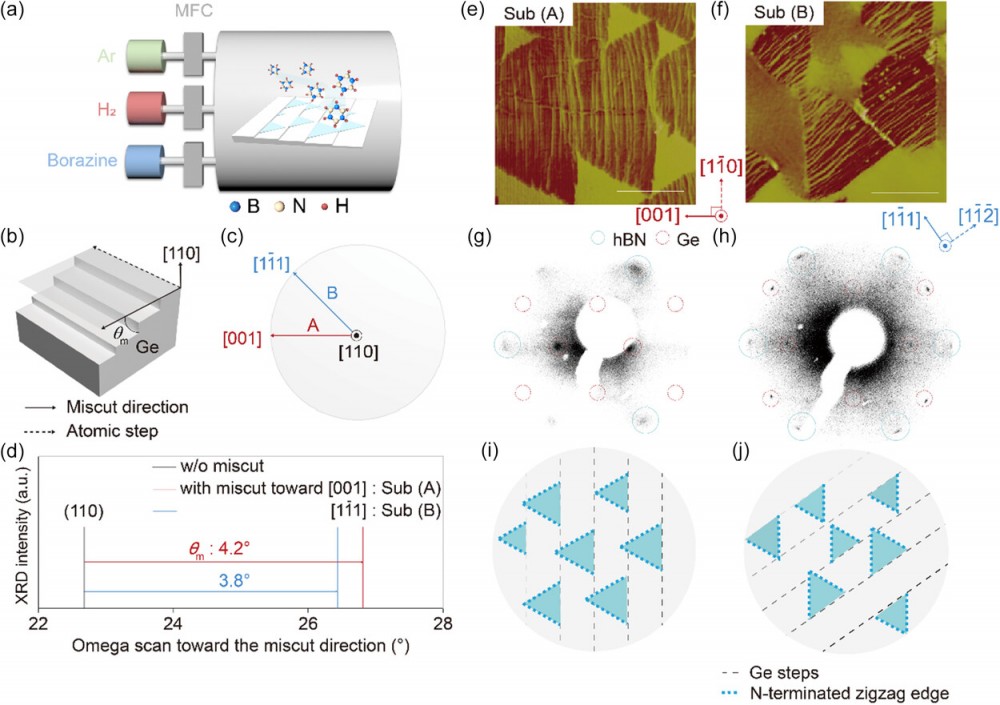
Insulating hexagonal boron nitride (hBN) films with precisely controlled thickness are ideal dielectric components to modulate various interfaces in electronic devices. To achieve this, high-quality hBN with controlled atomic configurations must be able to form pristine interfaces with various materials in devices. However, previously reported large-scale hBN films with uniform thickness either are polycrystalline or are not suitable for atomically clean assembly via mechanical exfoliation, limiting their applications in device technology. Herein, the large-scale growth of monolayer (ML) single crystalline hBN films on Ge(110) substrates by using chemical vapor deposition is reported. Vicinal Ge(110) substrates are used for the step-directed epitaxial growth of hBN, where Ge atomic steps act as the hBN nucleation sites, guiding the unidirectional alignments of multiple hBN domains. Density functional theory calculations reveal that the optimum hydrogen passivations on both hBN edges and Ge surfaces enable the epitaxial coupling between hBN and the Ge step edges and the single crystallinity of the final hBN films. Using epitaxially grown ML hBN films, a few hBN films with controlled stacking orders and pristine interfaces through a layer-by-layer assembly process are fabricated. These films function as high-quality dielectrics to enhance carrier transport in graphene and MoS2 channels.
Link : https://onlinelibrary.wiley.com/doi/10.1002/sstr.202400297


